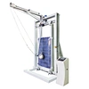


Model No: HT-2400
Solar panels PV Photovoltaic modules EL defect tester
The Solar Panels EL Tester uses electroluminescence imaging to detect hidden cracks, broken grids, and soldering defects in monocrystalline and polycrystalline modules. Ideal for PV production lines and labs.
Quantity :
The Solar Panels EL Tester uses electroluminescence imaging to detect hidden cracks, broken grids, and soldering defects in monocrystalline and polycrystalline modules. Ideal for PV production lines and labs.
I.Product Introduction
The solar panels EL tester is a high-precision detection device based on electroluminescence imaging technology, designed specifically for quality control of photovoltaic module production lines and laboratories. It quickly and non destructively identifies various internal defects such as hidden cracks, fragments, broken grids, black core pieces, and poor welding of solar panels by capturing microscopic images of the components when they are powered on and emit light. It is the core quality inspection equipment for improving the yield of solar panel products and ensuring product quality.
II.Functional Features
Excellent efficiency, stable and reliable:
The overall performance is superior, and unique technology is adopted to ensure high stability and efficiency.
Equipped with extremely fast testing speed, supporting 24-hour continuous uninterrupted work, meeting high-intensity production needs.
Reasonable structural design, convenient installation and maintenance, optimized configuration of various system components, and maximizing the efficiency of the entire machine.
Intelligent software, easy to operate:
Equipped with industry-specific control software, the human-machine interface is user-friendly, and the operation is simple and programmed.
Compatible with online detection: automatic barcode scanning, automatic file naming and saving, automatic control of constant current source, automatic classification and saving of results.
Provide powerful image analysis functions: double-click to enlarge and display subtle features, unique photo query function, convenient for defect detection and tracing.
Accurate detection, insight into the process:
Based on the principle of electroluminescence (EL), accurately locate various defects of solar cells (such as silicon wafer defects, diffusion、etching、printing、sintering process issues).
By observing and analyzing defect images, problems in the production process can be effectively identified, providing direct basis for process improvement.
Strong compatibility and wide application:
Suitable for mainstream solar cell technology, compatible with various types of solar cells such as monocrystalline silicon and polycrystalline silicon.
Large size testing capability (2500x1400mm), meeting the testing needs of mainstream large-sized components.
The front and back of the component are designed to be compatible (the front of the component is photographed downwards), suitable for pre - and post lamination inspection.
Related Products